Modeling the select delay of MUX in Verilog
I'm currently analyzing the timing behavior of an FPGA Look Up Table (LUT). These insights shall than be used to optimize the PPA of a Loop PUF, where each delay element is implemented using one LUT.
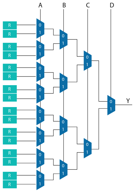
A LUT consists of binary tree of 2-input MUXs. Each LUT input port is connected to the MUX select ports at the respective level. The leafs of the MUX tree are connected to the configuration memory of the LUT. The final MUX at the tree root is connected to the output of the LUT.
The idea of a Loop PUF is to build a fingerprint out of the delays of a manufactured chip. Due to uncontrollable manufacturing variations these delays are unique to each chip. These can be used for authentication in a challenge-response manner.
To measure the response a signal is passed through a odd-numbered series of inverters that are connected in a loop. Each inverter adds his unique delay to the whole path. The output of the last inverter is fed back to the input of the first inverter. This creates a alternating signal. The alternations per unit of time depend on the unique path delay of the chip.
On an FPGA each inverter is implemented using one LUT. One LUT input is connected to the output of the previous loop element. The LUT output is connected to the LUT input of the next loop element. The other LUT inputs are used to modify the path taken by the signal through the LUT.
So far the analysis points in the direction that the signal delay is slightly different for different select signals. What is unclear whether there is some underlying trend, that would offer an attacker exploitable information.
One idea is to get further insight from modeling the MUX tree. The following Verilog code implements the basic building block of a LUT, a 2-input MUX, together with relevant delay properties for the select signal.
`timescale 1ns / 1ps

module mux2x1 # ( parameter D0 = 0, parameter D1 = 0)
    (
    input sel,
    input i0,
    input i1,
    output o
    );

    reg sel_w;

    always @(sel) begin
        if (sel == 0)
            sel_w <= #D0 sel;
        else
            sel_w <= #D1 sel;
    end

    assign o = sel_w ? i1 : i0;

endmodule
The corresponding testbench:
`timescale 1ns / 1ps

module tb_mux2x1;

    reg I0, I1, SEL;        // inputs to the DUT need to be driven
    wire O;                 // outputs from the DUT can be read

    parameter PATH0_DELAY = 1;  // use delays empirically measured
    parameter PATH1_DELAY = 2;  // use delays empirically measured
    parameter LOOP_DELAY = 10;  // use delays empirically measured
    parameter N_SIM_CYCLES = 5;

    // instantiate DUT   module(TESTBENCH)
    mux2x1 #(.D0(PATH0_DELAY), .D1(PATH1_DELAY)) m1 ( .i0(I0), .i1(I1), .sel(SEL), .o(O) );

    // alternating select signal of the Loop PUF
    initial begin
        SEL = 0;
        forever #LOOP_DELAY SEL = ~SEL;
    end

    // sim setup and finish
    initial begin
        I0 = 0;
        I1 = 1;

        #(N_SIM_CYCLES * 2*LOOP_DELAY + 5) $finish;
    end

    // check MUX select path 1 delay
    initial begin
        repeat(N_SIM_CYCLES) begin
            @(posedge SEL) begin
                #(PATH1_DELAY - 0.1) if (O == I1) $error("%t : Input %b should not have reached output yet, expected out = %b", $time, SEL, I1);
                #(PATH1_DELAY + 0.1) if (O != I1) $error("%t : Input %b should have reached output by now, expected out = %b", $time, SEL, I1);
            end
        end
    end

    // check MUX select path 0 delay
    initial begin
        repeat(N_SIM_CYCLES) begin
            @(negedge SEL) begin
                #(PATH0_DELAY - 0.1) if (O == I0) $error("%t : Input %b should not have reached output yet, expected out = %b", $time, SEL, I0);
                #(PATH0_DELAY + 0.1) if (O != I0) $error("%t : Input %b should have reached output by now, expected out = %b", $time, SEL, I0);
            end
        end
    end

endmodule